
http://picasaweb.google.com/FoxxOTG/TechCrapGizmos#5323705922529643682 Click the Magnify Icon for a larger size picture, for those of you that like those fine sexy details.
Some things I have been able to discover:
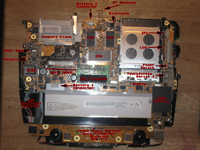
The FlashROM board itself has missing chips. It might be possible to retrofit a 512MB board to hold more. I would need someone to donate a 512MB board to me, and help from someone with a 1GB or higher board for comparison. The main FlashROM chip itself is a Samsung K9K4G08UOM - Datasheet here http://www.alldatasheet.com/view.jsp?Searchword=K9K4G08UOM
There is also a TDK GBDriver RA3 http://www.tdk.co.jp/tefe02/ew_002.pdf This chip turns the typical NAND FlashROM into an IDE device. This is the bugger that does all the magic. This reinforces my idea to rework a 512MB Board with more NAND Flashrom, but alas, I am not about to put my only FlashROM on the chopping block just yet.
There is a typical dual channel IDE bus, we know the FlashROM as HDD1, on the board is JHDD1. Notic I marked JHDD2 on the board under the compact flash slot. This looks exactly like compact flash header pads. Unfortunately there is no way to have a full size compact flash card installed even if this header is put back in place. The compact flash card slot on the board gets in the way. I would not risk removing it in any way... Although this does give us some options. Hook up a cable adapter into a CF header and decent size Microdrive/CF card, use a small iPod 30GB HDD, or hell, wire in a full 44 pin laptop HDD. Those are all options, the main issue is the lack of space. I have some parts coming in (I hope) so I might be able to take my iron to my board and let you know how hard each option would be, as I have all the spare drives already, minus a few adapter boards which I can get pretty easy and cheap.
I have no idea what SW1 does. It is a SPDT switch, I assume its for master/slave of the IDE2 chain. Once I get a drive installed (give me a LONG time) I will be able to tell. When this switch is put on its alternate setting, all I notice is my right speaker will hiss with what sounds like EMF from the system. *shrugs*
The BIOS is a typical SST 49LF002 Firmware Hub (FWH). Datasheets are YUMMY! http://www.datasheetcatalog.com/datasheets_pdf/4/9/L/F/49LF002.shtml
The Bluetooth is actually a Cambridge Silicon Radio (CSR) Bluecore 4 chipset. http://www.csr.com/products/bc4range.htm. This is a pretty bad-ass chipset. They are very reliable, hackable, linux friendly, and can even do some cool things under a linux OS. I am very familiar with this chipset under both windows and linux, and it can be very fun with a beefed up antenna. Ahhh yes, the Bluetooth Antenna... yes, it can be modified with a proper RF jack to allow a better rubber duck, or even directional 2.4GHz class antenna. Any of you that really know me, or poke around my picasa page know I do quite a bit of 2.4Ghz stuff. >:}
The system RAM is not safely upgradable. I would not risk it. The chips would need to be removed from the board. With the amount of surface mount devices in the local areas, it could risk damage or accidenal displacement.
From what I can tell, the Compact Flash is tied right into the USB 1.1 as an onboard USB Card Reader. This will make any OS install or loading from Compact Flash slow... painfully slow. I have been playing with it, I have not been happy with its performance.
Regarding USB 2.0... You should be able to add a PCMCIA USB 2.0 adapter, but this will add quite a bit of bulk, and I do not know if it would be bootable, or even detected by the BIOS. I have a PCMCIA USB 1.1 card, I will try that in a few days to see if the proof of concept is viable.
The bottom cradle connector is a typical gender bender setup. You can get standard pin headers and make yourself a breakout board to do as you please. I dont have a pinout right now, if anyone has it please post. Getting interfaced into this is very simple. Give me a little bit and I can do a how-to tutorial with pics if anyone is interested.
I will post more down the road, I just wanted to take this topic off.


